Mobile HBM: Empowering the Next Generation of Mobile Device Memory
With the increasing demand for computational performance and data processing capabilities in mobile devices, traditional LPDDR memory is struggling to meet the needs of increasingly complex applications. To address this challenge, a new memory technology, Mobile High Bandwidth Memory (HBM), has emerged.
What is Mobile HBM?
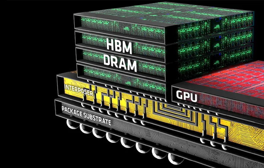
 Mobile HBM is a novel DRAM stacking technology designed to provide mobile devices with high bandwidth and low-power memory solutions. By vertically stacking multiple LPDDR DRAM chips and connecting them using high-speed interconnect technology, it achieves higher data transfer rates and larger capacities, bringing a new level of memory solutions to mobile devices.
Simply put, it's like a tall building where each floor is a DRAM chip. These floors are connected by high-speed "elevators" (TSVs) that quickly transport data from one floor to another. The "management center" at the top (control chip) directs the operation of these elevators, ensuring efficient and accurate data transfer.
Advantages of Mobile HBM
● High Bandwidth: Compared to LPDDR, Mobile HBM offers higher bandwidth, significantly improving the overall performance of mobile devices, especially in graphics processing and artificial intelligence.
● Low Power Consumption: Despite the increased capacity, Mobile HBM is well-controlled in terms of power consumption, meeting the power requirements of mobile devices.
● High Performance: Mobile HBM can accelerate AI computations on mobile devices, supporting various AI applications.
Implementation of Mobile HBM Technology
To realize Mobile HBM, Samsung and SK Hynix have developed different technical solutions. Samsung Electronics is currently developing a technology called "VCS," while SK Hynix is developing a technology called "VFO." These technologies aim to provide more IO data pins to effectively support performance improvements.
● Samsung VCS Technology: Through vertical interconnect technology, multiple DRAM chips are stacked to achieve higher I/O density and bandwidth. Samsung  plans to launch a new mobile memory, LP Wide I/O, in 2025, with a single-package bit width of 512 bits, 8 times that of LPDDR5 memory. The VCS advanced packaging technology offers 8 times and 2.6 times the I/O density and bandwidth compared to traditional wire bonding; compared to VWB vertical wire bonding, VCS technology has 9 times the production efficiency.
● SK Hynix VFO Technology: Combining FOWLP packaging and DRAM stacking, it shortens the signal transmission path and improves energy efficiency. VFO technology verification samples have reduced wire length to less than 1/4 of traditional memory, and energy efficiency has also increased by 4.9%. Although this scheme brings an additional 1.4% heat dissipation, the package thickness is reduced by 27%.
Applications and Challenges of Mobile HBM
Mobile HBM has broad application prospects and is expected to play an important role in many fields. Its high bandwidth and low power consumption make it ideal for flagship smartphones, AR/VR devices, and AI acceleration. In flagship smartphones, Mobile HBM will bring smoother gaming experiences, faster app launch speeds, and better multitasking capabilities. In AR/VR devices, Mobile HBM can provide more immersive virtual reality experiences. In AI acceleration, Mobile HBM can accelerate AI computations on mobile devices, supporting various AI applications. Moreover, HBM has already emerged in self-driving cars, such as Waymo, and is expected to become mainstream in the future.
However, the development of Mobile HBM also faces some challenges. First, the cost is higher compared to traditional LPDDR. Second, the manufacturing process of Mobile HBM is relatively complex and requires higher technical levels. Additionally, as the number of stacked layers increases, heat dissipation and reliability are also concerns.
Summary
Mobile HBM, as an emerging memory technology, has great potential. As technology matures and costs decrease, Mobile HBM will play an increasingly important role in the mobile device market, driving continuous improvements in mobile device performance and providing users with a better experience. However, to achieve large-scale commercialization, challenges such as cost, technology, and reliability need to be overcome.
Conevo Electronic Chip Wholesale
● NXP Processor MIMXRT1064CVL5B, a ARM Cortex-M7 core 32-bit processor, designed for applications requiring high computing power and real-time response. Up to 528MHz running speed, MIMXRT1064CVL5B support 32KB first-level instruction cache and 32KB first-level data cache, with excellent CPU performance and real-time processing capabilities.
● TI FRAM microcontroller MSP430FR6972IPMR, 16-bit RISC architecture MCU, supports clock frequencies up to 16MHz, providing efficient instruction execution capabilities. The MSP430FR6972IPMR integrates a 12-bit ADC and supports a wide supply voltage range from 3.6V to 1.8V for a wide range of power supply environments.
● ON Semiconductor MOSFET FDMS86101, FDMS86101N Channel PowerTrench MOSFET achieves extremely low on-resistance and maintains excellent switching performance for applications requiring fast switching. Combined with low rDS(on) and high efficiency, the FDMS86101 performs well in a variety of power conversion applications, such as power management, motor drives, and more.
Website: www.conevoelec.com
Email: info@conevoelec.com


