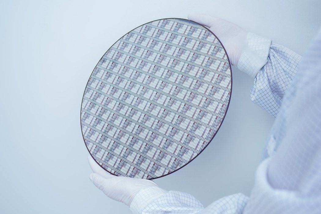
Infineon's Groundbreaking Innovation: The World's Ultra-Thin Silicon Wafer Tech
In today's increasingly competitive global semiconductor industry, technological innovation has become the key for major manufacturers to compete for market share. Recently, Infineon Technologies announced a significant technological breakthrough - the successful launch of the world's thinnest silicon power wafer, a milestone that not only marks another achievement for Infineon in the field of semiconductor manufacturing technology but also heralds a significant leap in power semiconductor technology.
Technological Breakthrough: 20 Micron Ultra-Thin Wafer
 Infineon's technological breakthrough is reflected in its successful reduction of the thickness of silicon power wafers to 20 microns (μm), which is nearly half of the 40-60μm thickness found in existing market wafers. These ultra-thin wafers have a diameter of 300 millimeters, equivalent to a quarter of the thickness of a human hair. By reducing the wafer thickness, Infineon has successfully halved the substrate resistance, thereby reducing power loss by more than 15%, which is of great significance for improving energy efficiency and reducing costs.
The new technology has a wide range of applications, especially in the field of AI. Infineon's integrated intelligent power stages (DC-DC converters) have adopted this ultra-thin wafer technology and have been delivered to the first batch of customers. This technology is particularly important for high-end AI server applications because it can promote vertical power transfer design based on vertical trench MOSFET technology, achieving a highly compact connection with AI chip processors, thereby increasing overall efficiency. In addition, this ultra-thin wafer technology will also be mainly applied to 12V devices, used for local power supply conversion of the next generation of AI GPUs, TPUs, and CPUs with vertical power, which require a large current of 1000 to 2000A at 0.8V voltage.
Market Impact: Competition and Cooperation
Infineon's technological breakthrough is expected to arouse great interest in the industry below 40V and has already conducted in-depth interactions with AI customers. With the entry of 20μm ultra-thin power semiconductor wafers into the market, Infineon is expected to expand its leading position in the field of power semiconductors once again. This technological upgrade also means that domestic power semiconductor manufacturers will face more intense competition. China is the world's largest power semiconductor market, contributing about 40% of the power semiconductor market. Although domestic power semiconductor technology has made significant progress, in the face of technological breakthroughs by international giants such as Infineon, ON Semiconductor, and STMicroelectronics, domestic manufacturers need to accelerate technological innovation and market layout to maintain competitiveness.
Technical Challenges and Solutions
To overcome the technical barriers of reducing the wafer thickness to 20μm, Infineon's engineers have established an innovative and unique wafer grinding method, which greatly affects the processing and processing of the back of the thin wafer. In addition, challenges related to technology and production, such as wafer warpage and wafer separation, also have a significant impact on ensuring the stability and first-class robustness of the back-end assembly process. The 20μm thin wafer process is based on Infineon's existing manufacturing technology, ensuring that the new technology can be seamlessly integrated into the existing large-scale Si production line without additional manufacturing complexity, thereby ensuring as high a yield and supply security as possible.
Conclusion
 Infineon's launch of the world's thinnest silicon power wafer not only demonstrates the company's innovative capabilities in the field of power semiconductor technology but also provides strong technical support for global low-carbon and digitalization trends. The successful application of this technology indicates that future semiconductor devices will be more efficient and energy-saving, and it also brings new opportunities and challenges for the development of related industries. In today's increasingly competitive global semiconductor industry, Infineon's technological breakthrough will undoubtedly lead the industry into a new stage of development.
Main Product of Infineon, Find In Conevo Distributor
1. BSR92P is a P-channel enhancement mode Field-Effect Transistor (FET) with a maximum drain-source voltage of -250V, offered in an SC-59 package by Infineon Technologies. It is characterized by low RDS(on) for higher efficiency, small package size for PCB space savings, and compliance with RoHS standards, making it suitable for a wide range of applications including automotive lighting, battery management, and motor control.
2. BSR202NL6327 is an N-channel enhancement mode MOSFET from Infineon Technologies, featuring a maximum drain-source breakdown voltage of 20V, a continuous drain current of up to 3.8A, and a compact SC-59 package. It is suitable for various applications requiring high efficiency and space-saving solutions, such as power management, automotive electronics, and industrial control systems.
3. The SS83PH6327 is a high-performance P-channel MOSFET designed for power management applications, offering a maximum drain-source voltage of -80V, low RDS(on) for efficient power conversion, and a compact surface-mount package suitable for dense PCB layouts. It is ideal for use in battery management systems, automotive electronics, and other applications requiring precise control and efficient power handling.
Website: www.conevoelec.com
Email: info@conevoelec.com


